Tentative TAs, and Office Hours:
- Tony Forzley: Thur 12:00-1:00 (?) room ME 5137, this is a room
inside of the Blue
Room, ME 5138 tforzley{at}doe.carleton.ca
- Saber Amini Tue 1:00-2:00 (?) ME 5138 (Blue Room)
samini{at}connect.carleton.ca
Office Hours for Prof. Plett
- I am at Carleton every day, so you are welcome to come see
me any time I am there, (but preferably not just before one of
my lectures). Good times would be Tuesday morning, 11:00-12:00
or Wednesday afternoon 2-3.
Exam Reveiw Sessions:
- Wed. Dec 12 2:00-4:00, ME4124
- Thurs
Dec 13, 2:00-4:00, ME4124.
Final Exam Friday December 14, 9:00-12:00, Fieldhouse
Final Term
Marks Including Assignment 3 Updated Nov
30, 2007
Please make sure your marks have been recorded correctly. For
those who have not done a particular assignment, there may still
be some opportunity to do so, in order to get some of the marks
(obviously there would be some late penalty), but more importantly,
to go through the exercise in preparation for the final exam.
Please contact me for more information.
Updated Oct
29, 2007 List of Changes between 2006 and 2007 course notes (mostly
complete including labs, now including Assignments 2 and 3, Exams
2004, 2005, 2006 and answers.)
I have checked the 2004 notes and they are nearly
the same as the 2006 notes - the further differences are minor
(missing the extra page 1b of system information, transistor
noise sources are not listed, p. 29, conversion from parallel
to series in tuned amplifier example has the wrong final answer
- Zs should be 62.89 - j790.5. Also the 2004 notes do not have
the extra page on I, Q modulation, but it is in the 2006 and
2007 notes right after the section on AM, just before the section
on FM Radio.)
Of course, the lab has different numbers (the correct 2007 numbers
can be found in the above
link) and the exams at the back are older. I also note that prior to
2007, the course notes did not include assignments 2 and 3. These can
be posted, or extra copies handed out to individuals who need them.
Assignment 3 Info
Due 4:00 in class Wednesday, Nov 28 (our second last class)
Latest Comments
- The closed-loop pulse to start up the oscillations is already
there. If it works (the oscillations start up) there is no need to
modify it.
- The output waveform is expected to be non-symmetrical, that
is, the negative peak is different from the positive peak. This
is because of non-linearity. Without nonlinearity, the oscillation
amplitude would keep on growing. Now the amplitude is limited
by the transistor saturating, and this flattens the lower portion
of the waveform.
Comments
-
Assignment 3 is a simulation done on your own and singly. However,
since we have odd weeks reserved for labs, you might wish to
work on the assignment during your regular lab time on Nov 21,
22, or 23. We plan to have a TA available in the computer room
on those days, from about 10AM.
-
Assignment 3 is found on pages 153 and 154 of the 2007 course
notes. For those using 2006, 2004 or other notes, assignments
have now been posted above in the "Changes" document.
You will need to copy and modify the following two programs for
oscillator analysis. Your aim will be to achieve a particular
output frequency and power, and being approximately impedance
matched. So, what you will need to change:
-
Frequency determining components: C1, C2 (LT is given)
-
Load Resistance: RL
-
Resistor to represent transistor output resistance: RE4
(For open loop only)
-
Open loop: Frequency Range in .AC command to center on your frequency,
optimize curves
- Closed Loop: Time range in .TRANS command to show rise time,
maybe zoom in to show a few periods to allow frequency to be
calculated. Make sure where you zoom in, the output voltage
is completely settled.
- Note instructions say to feed in a pulse to start the
oscillations - this is already in the SPICE file, so no further
changes are needed.
Reporting: this list may not be complete but you will need at least:
-
Your frequency of oscillation based on your student number
-
Bias calculations (no design) All transistor voltages, bias current,
re and gm.
-
Determination of RL to achieve required output power (estimating
voltage swing).
-
Calculation for C1, C2 to set frequency and impedance matching.
-
Open loop ac simulation results, clearly labeled plots showing
magnitue and phase of loop gain (not gain to the output but loop
gain). From this can determine
-
predicted frequency of oscillation compare to calculation above,
discuss any differences.
- gain margin, compare to theory, discuss and differences.
-
Closed loop results, clearly labeled plots showing time domain
response. Will probably need at least two plots, one showing
overall shape, one zoomed in after the waveform has settled.
Determine:
-
startup time (define how you measure it)
- Amplitude of oscillation, compare to prediction, discuss
- actual frequency of oscillation, compare to calculation and open
loop prediction, discuss. Note using an FFT is useful to double-check
the frequency you calculated from the waveform.
Assignment 3 Example SPICE file for Open-Loop Oscillator test.
Assignment 3 Example SPICE file for Closed-Loop Oscillator test.
Assignment 2 Info
Questions
(in red)
and Answers
(in blue)
-
For Question 5, how exactly am I supposed to solve for the frequency
range for which phase error remains less than 0.3?
I'm not sure about "exactly", but the fast answer is to use the
equation in the course notes for phase error versus frequency,
or use the plot of this equation, also provided in the course
notes. In the notes, that equation was solved to find the miximum
phase error and this resulted in a simplified formula, but obviously,
this can only be used to find the maximum phase error. Any other
phase errors requires that you use the full equation or the plots.
Note, that it is probably not possible to solve the full equation
analytically for a particular phase error, but will instead have
to use an iterative technique (e.g., guess or use the curve to
estimate the required frequency, calculate phase error, see if
it is too big or too small and use that to refine the estimate
for frequency, etc.) Simply using the given plot will be faster,
but less accurate, especially if you discover you have a damping
constant for which there is no curve.
-
Regarding question, for the minimum step that will break lock,
is the given max error (pi/4) enough to break lock or do we use
the maximum input phase difference of the phase detector (pi)?
You assume that nominally you are operating in the middle of
the range, hence you can only have a phase error of half the
complete range, or pi/2, to take you right to the edge.
-
I am not getting a Kvco close to the suggested value in the assignment.
Should I do my measurements again?
No, those values were for the old version of the PLL Chip. For
this year's IC, if you set the frequency to be about 1.2 MHz
at 4V Kvco is estimated to be about 2 pi x 1.2 Mrad/s/4V or about
2 Mrad/sec/V.
-
In deriving the filter transfer function, what do we do about
the input connected to 2.5 V?
For small signal analysis, voltage sources are always considered as AC
ground. Compare this to the analysis of transistor amplifiers where
bias voltage, VCC, etc become grounds. This is equivalent to saying
that we are solving for the deviation away from the nominal voltage,
and the nominal voltage in this case is 2.5V.
-
I have 4 unknowns but only 2 equations - help.
Actually, there are 4 unknowns and three equations (one for gain
which at low frequencies should be 2, one for natural frequency,
one for damping). You will need to set one first, then solve
for the other components. E.g., limit resistor sizes preferably
from a minimum of a few hundred ohms to a maximum of a few hundred
k ohms, and even more ideally to no more than 100k and no less
than 1k. Also, you might wish to start with a standard capacitor
value, then calculate your resistors. Note that once you find
one set of values, you don't ever have to do these calculations
again, even if you don't like your values. All you need to do
is scale the values - for example, if the capacitor is scaled
by X then all resistors should be scaled by 1/X. So, start with
any value, e.g., R3=47k. Solve for the rest. Do you like the
resulting values? If not, scale capacitor by X, resistors by 1/X.
- I am getting an equation with negative values, I suspect because
my filter transfer function has a negative value - is this OK?
No, if one of your terms in the denominator is negative, this
means poles could be in the right half plane and the system would
be unstable. If the filter has a negative sign, then in order
to have negative feedback, the phase detector positive input
must be used. With a positive input on the phase detector, the
generic block diagram transfer function becomes FG/(1-LG) instead
of the previous FG/(1+LG), where FG is forward gain and LG is loop
gain.
More Assignment 2 info
-
Assignment 2 is found on page 152 of the 2007 course notes.
For those using 2006, 2004 or other notes, assignments have now
been posted above in the "Changes" document.
- Due date is Monday Nov 5 in class, the last lecture before
the second part of Lab 3, which starts on Wednesday Nov 7.
-
Please record your component values from the assignment as you
will need these to design your loop filter in the lab.
Lab 3 Info
Lab 3 Tentative, Approximate Marking
Scheme from 2006, probably close to the final value but subject to small
changes. (pdf)
Part 1
-
All ICs on the board are new, so there is no longer any problems with
them not being able to operate at the correct frequency (so ignore
this comment in step 5)
- The PLL chip is also new, and the VCO characteristic has changed
(Data Sheets are posted with location as described in the lecture)
VCO design should be changed - now aim for about 1.2 MHz at Vc
= 4V. The characteristic will be very nearly linear with a slope
of about 300 kHz/V.
-
Lab 3 will be due after the second part of the lab has been done.
-
Lab Day Wednesday, Due Monday Nov 19
-
Lab Day Thursday, Due Tuesday Nov 20
-
Lab Day Friday, Due Wednesday Nov 21
Lab 2 Info
Short Q and A for Lab 2
Questions in red,
Answers in blue
-
Oct 21. How can I determine absolute amplitude from the fft plot?
I don't know of an easy way, hence I only use the fft function
in the 4505 lab to determine the freuqencies of the sidebands
and the relative amplitudes (preferably on a dB scale) of the
two sidebands, e.g, when filtering, or to tell how much lower
the carrier feedbthrough is than the sidebands.
On most dedicated spectum analyzers, there is a reference level
somewhere on the screen, e.g., - often 0 dBm is at the top of
the screen , then you count down by 10 or 20 dB per division,
but such a reference level does not seem to be available here.
The only way I would believe is if you calibrated it yourself
with a knwn amplitude. Instead, the experimental amplitudes are
determined from the time domain plots and the theoretical amplitudes
from the known input levels and gains.
-
Oct 18. How can I tell whether to use low level or high level
equations?
By the amplitude of the carrier.
Check Figure 11. If the curve is flat, (output is independent of
carrier amplitude) then it is high level. If the output is
proportional to the carrier level then it is low level.
-
Oct. 18. Do I need to know inductor Q?
Yes, for the last part, you will need to measure the Q of the
inductor in order to determine the parallel resistance which
is a dominant component in the gain calculation. If you did not
measure it during the lab, and if you still have your inductor,
you can still measure it using the meter in the lab. (The meter
is next to the lab exit door, next to computer room 4166). Make
sure to measure it at the highest possible frequency (100 kHz)
then scale the Q to your operating frequency (900 kHz) estimating
Q to be proportional to the square root of frequency. If you
have already returned your parts, you will have to estimate the
Q value and state that you estimated it (typical numbers are
17-20 at 100 kHz).
-
Oct. 18. My calculated gain is much higher than my measured gain - what
did I do wrong?
We have seen calculated gains up to a factor of 2 higher than
measured gain. There are a number of sources of error, each of
which reduces the gain. For your report, you should try to list
some of these sources of error.
-
Oct. 18. Do I need to know the output impedance
of the mixer?
You should know this in order to calculate gain for the last part -
e.g., similar to what you did for lab 1, the final value of R
is the parallel combination of your load resistance (50k), the
mixer output resistance and the inductor parallel resistance. The data
sheet gives ro, but only for high frequencies - you can assume
the low frequency ro is at least as high - it it wasn't I would
assume they would have shown it.
-
Oct. 18. My tuned circuit frequency was off
by 200 kHz, should I go back and modify it?
No. 200 kHz is a lot, and it would have been quite easy to adjust
values to get closer to the desired frequency. However, the important
thing is that you understand how a tuned circuit can be used
to filter one of the sidebands. So, as long as you have adjusted
your carrier frequency so that you can demonstrate that you can
filter either sideband then that should be OK. If I saw this
in the lab, I would say choose a smaller capacitor (to change the
frequency by +20%, you need roughly -40% change of capacitor
value since frequency is inversly proportional to the square
root of capacitance). But now that you are writing it up, don't
bother to change it if you have taken all the approprate measurements
and screen captures.
Lab 2 Due dates
- If your lab day is Wednesday, due on Monday Oct 22, 4:00
- If your lab day is Thursday, due on Tuesday Oct 23, 4:00
- If your lab day is Friday, due on Wednesday Oct 24, 4:00
Extra Notes for Lab 2 - written by
Tony in 2006 - we are not sure yet who will be marking this lab. (PDF)
Lab 2 Marking Scheme (PDF)
From an earlier year - This may not be quite the same this year,
but it should give you an idea of what is being looked for.
Inductor Q at 100 kHz and 1.2 MHz.
(Inductors are not yet finalized for 2007 - this is from 2006)
From results, we suggest you use the 33 uH inductor to get the
highest parallel resistance. In the lab you can measure Q at
100 kHz, then estimate Q at 800 kHz by assuming Q is proportional
to the square root of frequency.
At the end is a plot showing how the filter affects gain.
SPICE File For mixer
This is not required for the lab, but you may find it interesting
and useful. Note, this is a nonlinear circuit, so simulations
are in the time domain. Tos see output spectrum including harmonics
and intermodulation components, run the fft on the output transient
waveform. Note that for this simulation, discrete 2N3904 transistors
have been used, but in spite of this, the results are quite realistic.
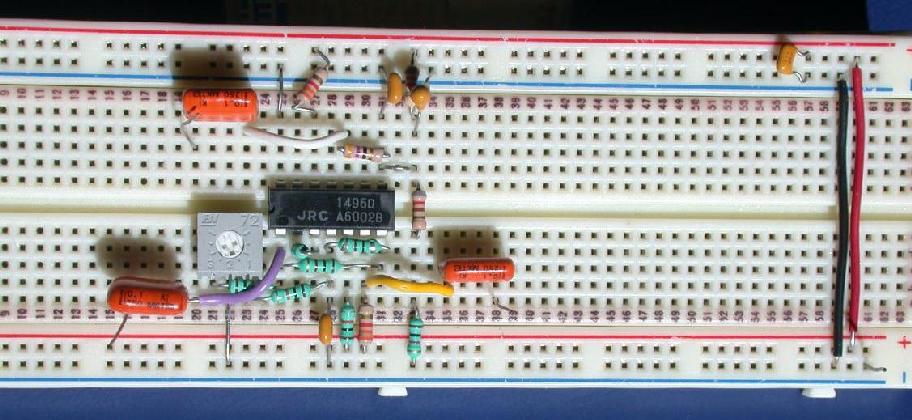
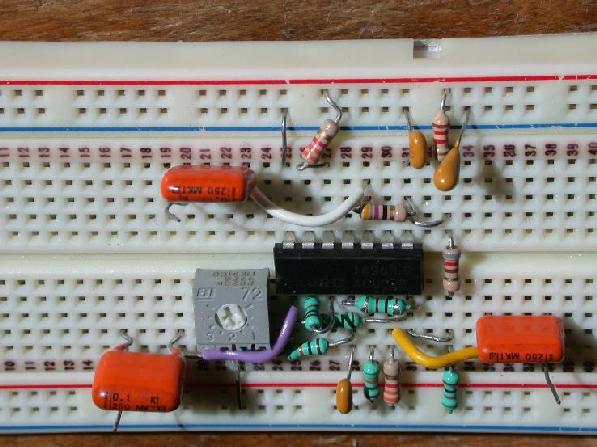
Photo of a Neatly Constructed
Mixer Board. Note that pin 7 has been used as an interconnect
point. It is labelled on the diagram as NC for No Connect. Often
it is not a good idea to use such pins, but in this case it seems
to work. (I still wouldn't do it though.) Also, note the yellow
wire hides a connection. Don't believe it?
Check out this picture from a different angle.
Lab 2, Mixer: Important Points:
-
Do construction ahead of time, if possible to save about one
hour of lab time.
-
Bring your breadboard, wire strippers, in case modifications
are needed, and mini screwdriver for adjustment.
-
Bring a floppy to store measurement results from scope. Note at some
stations, the scopes are connected to the computers so plots may be
saved directly.
Note that some of course content that we have
been covering in the first few lectures will not be part of the
final exam. For example, we will not ask you to do calculations
of transistor noise sources in final exams. This information
was provided just so you are aware that there are various noise
sources in communications circuits,
Lab 1 Info
Relationship of Assignment 1 to Lab 1
Note that Assignment 1 is to be done at the same time as Lab
1 or after you have done the first part of lab 1. At the very
least what you need from lab 1 is the value of the load resistor
and the input impedance of the tuned amplifier. Then, for assignment
1, you will add transformer based circuits to replace the load
resistor with a 50 Ohms load, and at the input you will add a
transformer-based matching circuit. After lecture 2, we have
not yet covered the material needed to be able to do the lab
or assignment. But, if you would like to get started with it, you
would need to look ahead in the course notes, and at the examples
posted on this web page directly below labeled Lab 1 Info.
Comments
-
After matching, the peak frequency will shift downwards a bit. Do not
readjust for this, but take your measurements (for matching, noise,
gain) at your previous centre frequency, we assume at approximately
9 MHz.
- Labs are now due after Thanksgiving Monday as follows: (make sure
it is done early enough so it doesn't interfere with preparation for
lab 2)
-
Lab Day Wed, Due Tue Oct 9
-
Lab Day Thur, Due Wed Oct 10
-
Lab Day Fri, Due Thur Oct 11
Lan 1 will formally only start in week 3, however, you can
work ahead if you like, using Carleton computer rooms, or PSPICE
on your own computer (the student version of PSPICE is sufficient to do this
lab and can be downloaded from the link below).
For those trying to get a head start, the template spice file is the
following:
SPICE File For Lab 1.
there is lots of information in the following tutorial style file:
Lab 1 Information, with Pictures, Sept 26, 2006,
Lab 1 will be held in Computer Room, next to hardware lab, ME4166
Lab 1 Approximate Marking Scheme 2005,
(PDF)
(similar to 2006, except specs are different, e.g., frequency,
bandwidth etc. Note, FFTs are not required for
2007)
Assignment 1 Info
- Assignments are due in class Wednesday Oct 10, at the beginning of the
class at 4:05.
All labs are done in groups of 2,
but Assignments are to be done individually
Assignment 1 Example.
Very speedily dashed off example solution to Assignment
1, but done for centre frequency of 1 MHz, bandwidth of 325 kHz,
following the lab 1 info posted earlier. If you find errors in
this, let me know.
-
You may choose to use Zin either from your calculations, or from
the simulation. These are known to be quite different because the
value stated for Cbe (Cpi) in the lab manual is quite a bit off
(it is listed as being 8 pF, but if you examine your SPICE output
file you will see a value more like 30 pF is used in the simulation).
PSPICE Student Version, exe file (28M) Note, this exe file
will unpack a few files. By default, it unpacks them in some
strange location, hard to find, so it is suggested you change
it to a known directory. Then you need to run the setup.exe file.
Click
here to request or download the 683MB OrCAD 15.7 Demo CD which
contains PSpice A/D. Direct from OrCAD
Note: the 28M version in the previous link is an older version of
PSPICE, but it will still do the job)
Link to the year 2006.
Link to the year 2005.
Link to the year 2004.
Link to the year 2003.
Course Objective
To learn about the design of
communications circuits. In other courses, the block diagram
approach has been used but in this course the emphasis will be
on the actual circuitry which makes up these blocks. Examples
of such blocks are tuned amplifiers, mixers, oscillators, phase
shifters and detectors. Communications systems considered are
AM, FM, television and telephony. Use of the PLL will be discussed.
Course Content
- Introduction to Telecommunications:
Components of a radio systems; noise, distortion impedance matching.
- Mixers and Modulators:
- Phase-Locked Loop and Applications:
Introduction to PLLs and applications such as:
synthesizers and FM demodulation.
- Oscillators:
- Frequency modulators and demodulators:
- Television Systems:
Transmission of intensity, color, retrace, blanking, and sound;
generation of the video signal, conversion of the video signal
to picture and sound. Other topics may include high-definition
TV, stereo sound.
Labs
Simulation Labs and Hardware Labs - Groups of 2, one writeup
per group, due one week after the scheduled lab day, 4:30 PM.
- Tuned Amplifiers: (Dates tentative)
(September 26, 27, 28 Simulation Lab. Use of a bipolar transistor
and some passive components to build a tuned amplifier operating
at about 10MHz. You will learn about use of transistor parameters,
tuned circuits and impedance matching.
- Mixers and Modulators:
(October 10, 11, 12) Use of an analog multiplier on an IC to
build frequency changers.
- Phase-Locked Loops:
(October 24, 25, 26 and November 7, 8, 8) Use of a commercially
available package to build a tracking filter, a synthesizer and
a an FM demodulator. The IC contains a voltage-controlled oscillator
a phase detector, and amplifiers. In this lab, the VCO and phase
detector will be characterized, then a complete phased-lock loop
will be built. The main external components will consist of a
simple loop filter and a divider to realize the synthesizer.
Marks:
a) Three assignments worth 5% each
b) Three Labs worth 10, 10,15 (about 20% for demo)
c) One written exam worth 50%.
**** Students must get at least 35% in the final exam. ****
Text:
There is no official course text. The printed course notes should
provide enough material, or some of the references can be consulted.
References:
- Smith,
"Modern Communication Circuits", Second Edition McGraw-Hill 1998, TK6553.S5595
- Krauss, Bostonian, Raab,
"Solid State Radio Engineering", Wiley 1980, TK6553.K73
- Rogers and Plett,
"Radio Frequency Integrated Circuit Design", Artech House 2003
- Hagen,
"Radio Frequency Circuit Design", Cambridge Press, 1997
- William F. Egan,
"Frequency Synthesis by Phase Lock", 2nd Ed. John Wiley & Sons,
2000
- Van der Puije,
"Telecommunication Circuit Design", Wiley 1992, TK5103.V
- Sinnema, McPherson,
"Electronic Communications", Prentice-Hall 1991, TK5101.S537
- Sedra, Smith,
(for intro to tuned amplifiers, oscillators)
- Stremler,
"Introduction to Communication Systems", (or other intro texts)
- Signetics,
"Linear Data Manual Volume 1: Communications", 1987
For Prof and TAs only: Password Required (jpg)
For Prof and TAs only: Password Required (board)
For Prof and TAs only: Password Required (L3)
For Prof and TAs only: Password Required (AppN)
For Prof and TAs only: Password Required (App)