When the ELEC4609 layouts are received, they are first processed to minimize the number of rectangles required to cover the pattern area. The designs are then placed in an array to form a multiproject chip containing all the class projects. The multiproject chip also includes test transistors (some with much smaller lengths than allowed in the projects), ring oscillators, and structures to measure the sheet resistance of the different layers.
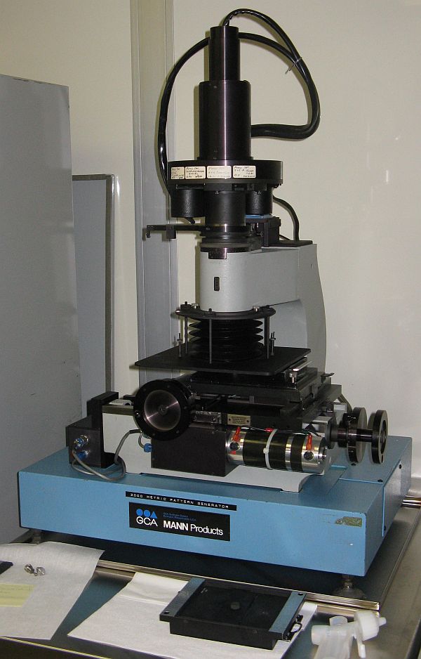
Each colored layer in the multiproject layout is printed on a high-resolution black and white photographic plate called a reticle . This is done using a pattern generator - in our case a David Mann 3000 pattern generator donated to us by Agilent. The pattern generator focuses light from a Xenon flash lamp (very similar to those found in cameras) through an aperture of computer-controlled height and width onto the photographic plate. The computer also positions the plate to the correct location in the x-y plane. Each box in the layout translates to an exposure on the plate. The reticle for the metal (blue) layer is shown here . The patterns on the reticle are 10 times larger than those which will be printed on the chip.
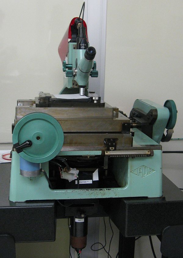
A step-and-repeat camera is used to optically reduce the reticle by a factor of 10 and repeat it approximately 100 times in the x-y plane to create the photomask that will be used to contact print the pattern on a silicon wafer. A magnified view of the photomask is shown here .
Commercially, all photomasks are now made by systems that write a focused electron beam. The smallest feature size that can be achieved with the black-and-white photography technique we use is about 1 micron, while chrome masks can produce dimensions below 100 nm.
To inspect the photomasks after they are generated, the d-well layer is first etched into a layer of oxide. The patterned d-well wafers are then re-coated with photoresist and the masks for poly, contact or metal printed. These test wafers can then be checked for defects and to ensure level-to-level registration is correct. Student volunteers are extremely helpful in carrying out these inspections. Photomask making began today with the generation of the device well reticle.
On Feb 17 test enclosed geometry nMOSFETs built on fragments of the SOI wafers being used in the multiproject chip fabrication completed processing. These samples allow VTn to be measured. Results suggest VTn is somewhat higher than expected (600mV rather than 300mV). This should help reduce leakage in the pass gate in the dynamic digital projects, but may upset the bias points for the analog circuits. More testing on these samples will continue next week.