ELEC 4609 WINTER 2017
EXAM PREPRATION
The best way to prepare for the ELEC4609 exam is to work through as many old exams as possible.
There will be a question-and-answer session on old exams in ME3269 Wednesday April 19 starting at 1:30PM.
PROJECT TESTING
A list of items to test is available here .
A brief report on testing is due April 15. One report per group is sufficient.
The report should include a brief description of the test set-up and how testing was done,
present waveforms captured, and compare to SPICE simulation where appropriate.
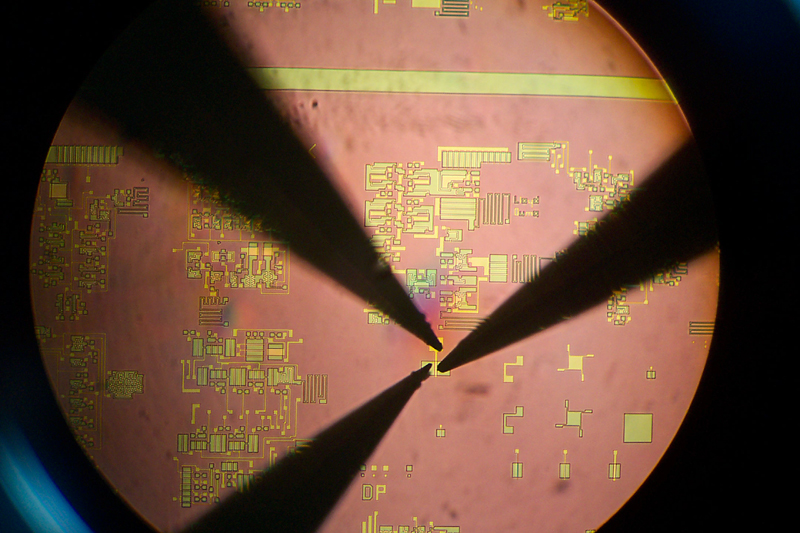
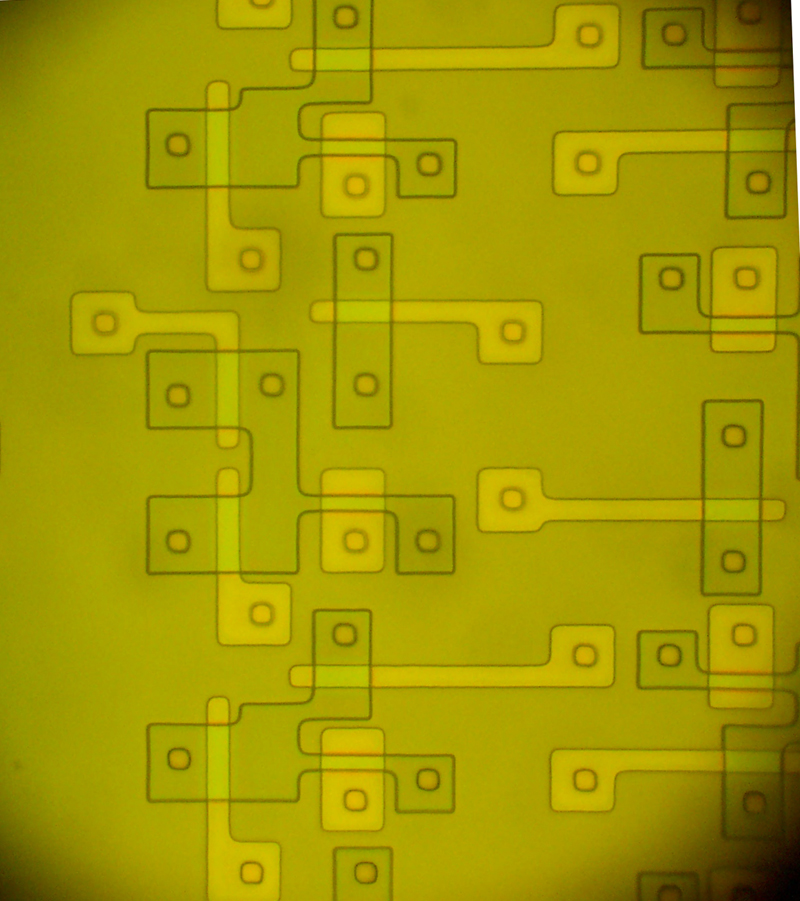
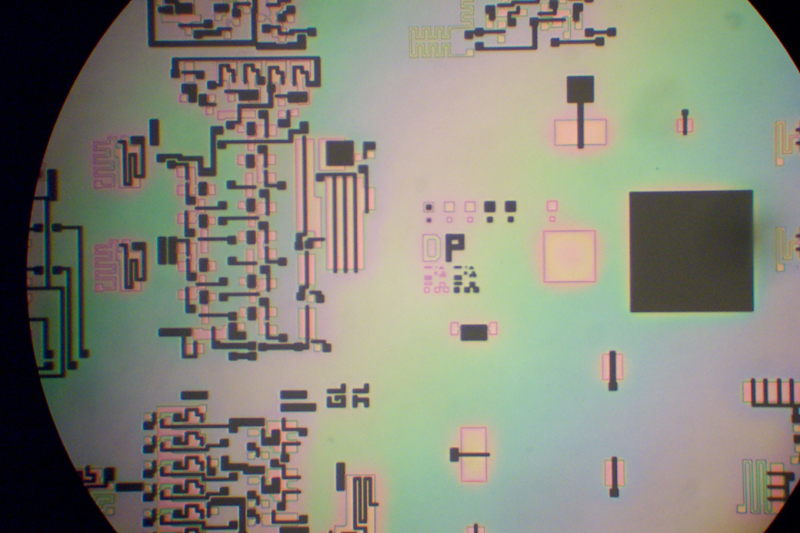
CHIP PHOTOS
Available here.
PRELIMINARY TEST RESULTS MAR. 27
Static PRSG:
1/1 working
Dynamic PRSG:
10/16 working (counting correct sequence).
1 shows flashes of some sort of PRSG sequence, but is unstable.
Of those not working, 1 has inputs shorted to VSS by input protection devices (this can probably be solved by microsurgery),
and 1 has no feedback connection (!)
3-bit counters:
1 out of 2 working
op-amps:
4/5 showing good DC transfer characteristics with small input offset and high gain
A to D converter:
1/1 working (linearity not tested)
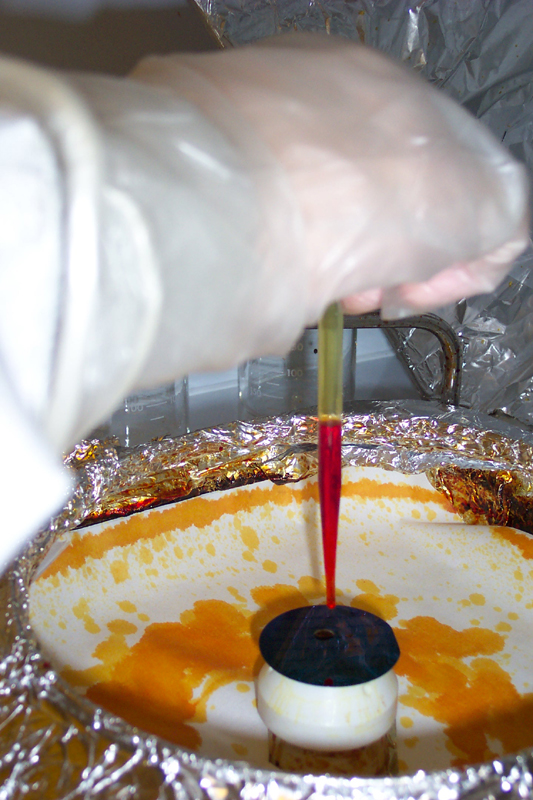
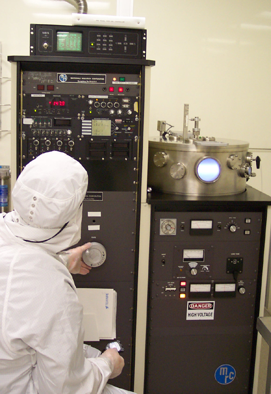
CHIP FABRICATION NOTES MARCH 23
Three wafers have now complete processing (one from each p-well dose).
The lightest dose is giving excellent nMOS and pMOS characteristics with low
subthreshold leakage when a small bias is applied to the substrate.
Many thanks are due to Microfab technical staff Angela McCormick, Rob Vandusen and Rick Adams,
whose dedication, hard work and skill have once again delivered working silicon for ELEC4609.
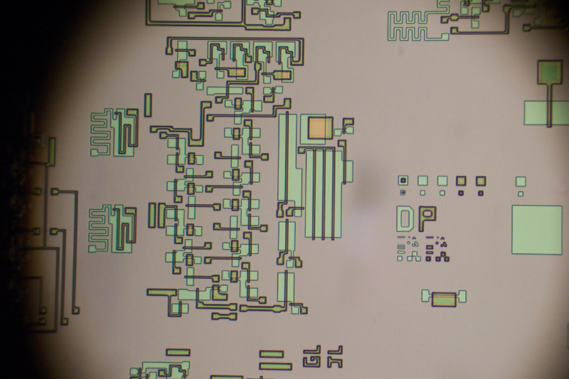
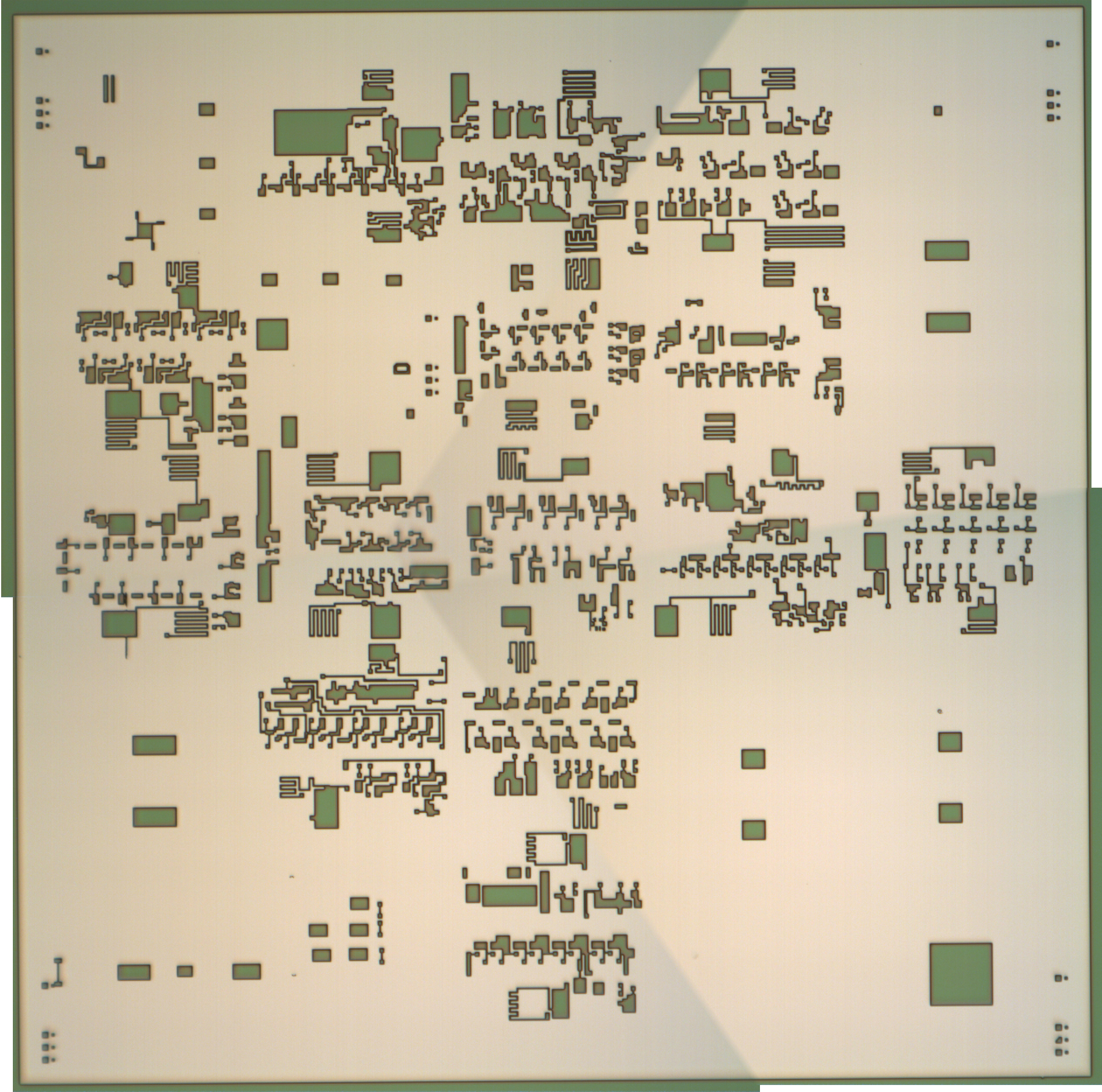
Here is a photo of a typical project after metal,
and here is a photo of the complete chip.
nMOS test device subthreshold characteristics
nMOS drain characteristics
pMOS subthreshold characteristics
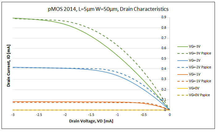
pMOS drain characteristics
For older reports see the fab blog archives .
IC DESIGN PROJECT REPORTS DUE MIDNIGHT TUESDAY MARCH 21
Individual reports are required. Submission is via CULearn.
Penalties for late submission will be significant after March 23.
Digital report guidelines
Analog report guidelines
LAB 3 BEGINS FRIDAY MARCH 17
Lab 3 will be covered in the next four formally scheduled lab periods.
Attendance is not compulsory but this material will be on the final exam.
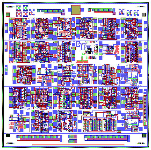
MULTIPROJECT CHIP ASSEMBLY COMPLETE
The multiproject chip LEdit file can be downloaded here . Please check to make sure that your layout has not been
corrupted by the rectangle optimization processor. Photomask preparation is now nearly complete. A .gif image of the chip is available
here .
IC DESIGN PROJECT SPECIFICATIONS
IC DESIGN PROJECT DEADLINES 2017
- January 12 Project sign-up (register on CULearn with partners' names, emails, proposed project)
- January 24 Full circuit schematic and SPICE simulation results due
- February 14 Final verified layout due
- Mid-March Comprehensive report on design due (individual reports!)
- Early April Brief report on test results (if fab run successful)
PHOTO GALLERY
Overview:
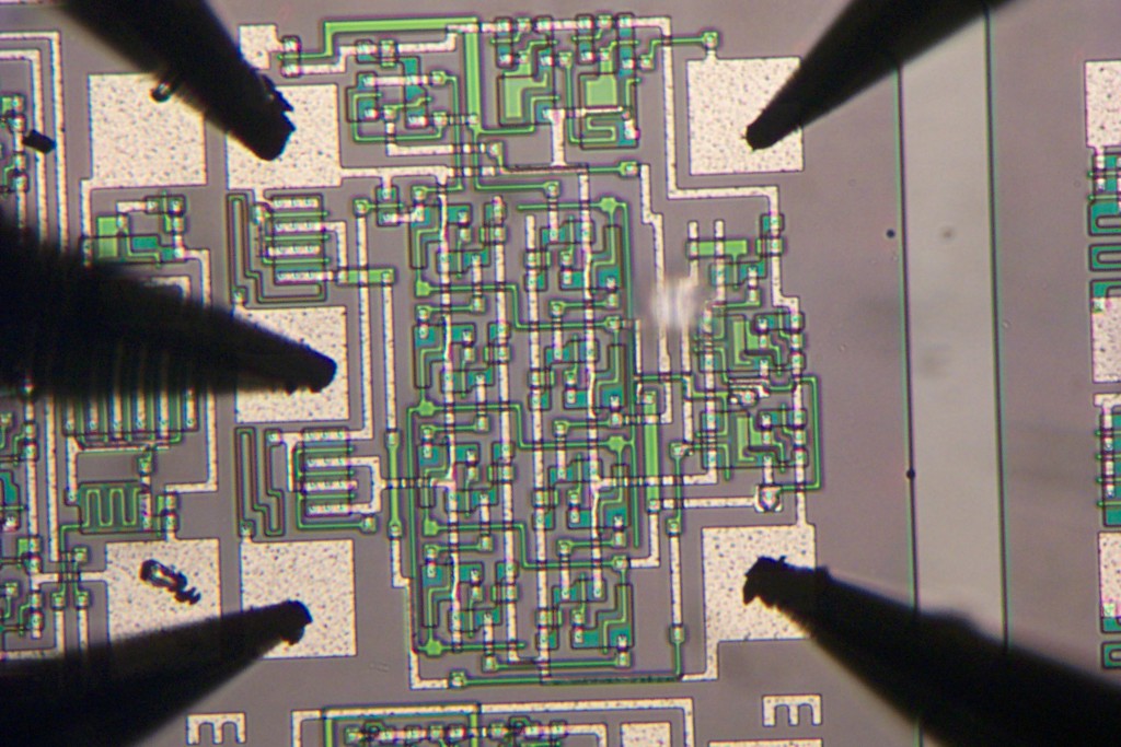
Chip photomicrographs:
Photographs relating to microfab activities:
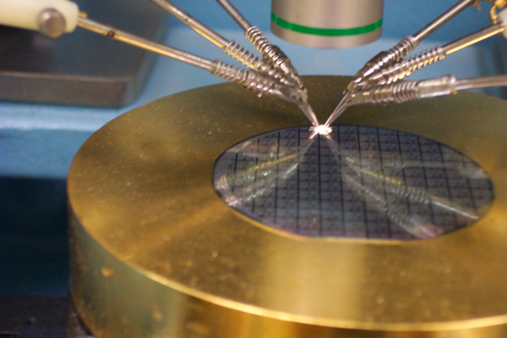
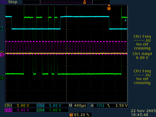
Pictures of circuit testing on prober:
Test MOSFET characteristics compared to models:
MICROART GALLERY
here